DRAWING NO. ES-01 · REV 2026

Erik Sunden

Mechanical Engineer — Robotics, Automation & Product Development

Eighteen years taking hardware from a sketch to something that ships — nail-painting robots, carbon-fiber print heads, quantum-dot deposition systems, and the tooling behind them. Based in the San Francisco Bay Area since 2006.

SF BAY AREA 18+ YRS EXPERIENCE 4 US PATENTS GEORGIA TECH, M.S. / B.S. ME
Erik Sunden
E. SUNDEN
SHEET 02 / 06

Selected Work

Self Employed at Sunden Design LLC

Fairfax, CA CURRENT

Clockwork

Founding Mechanical Engineer · 2018–2025 · San Francisco, CA

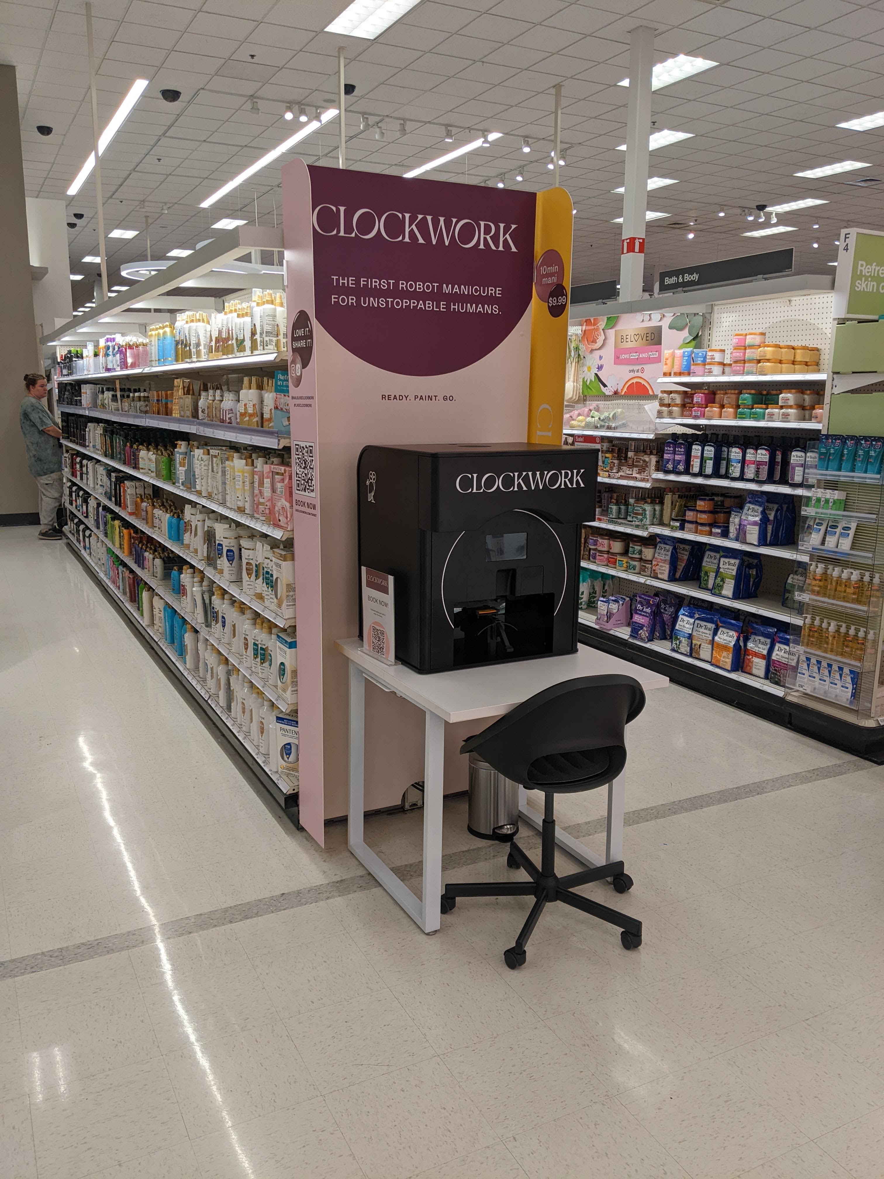
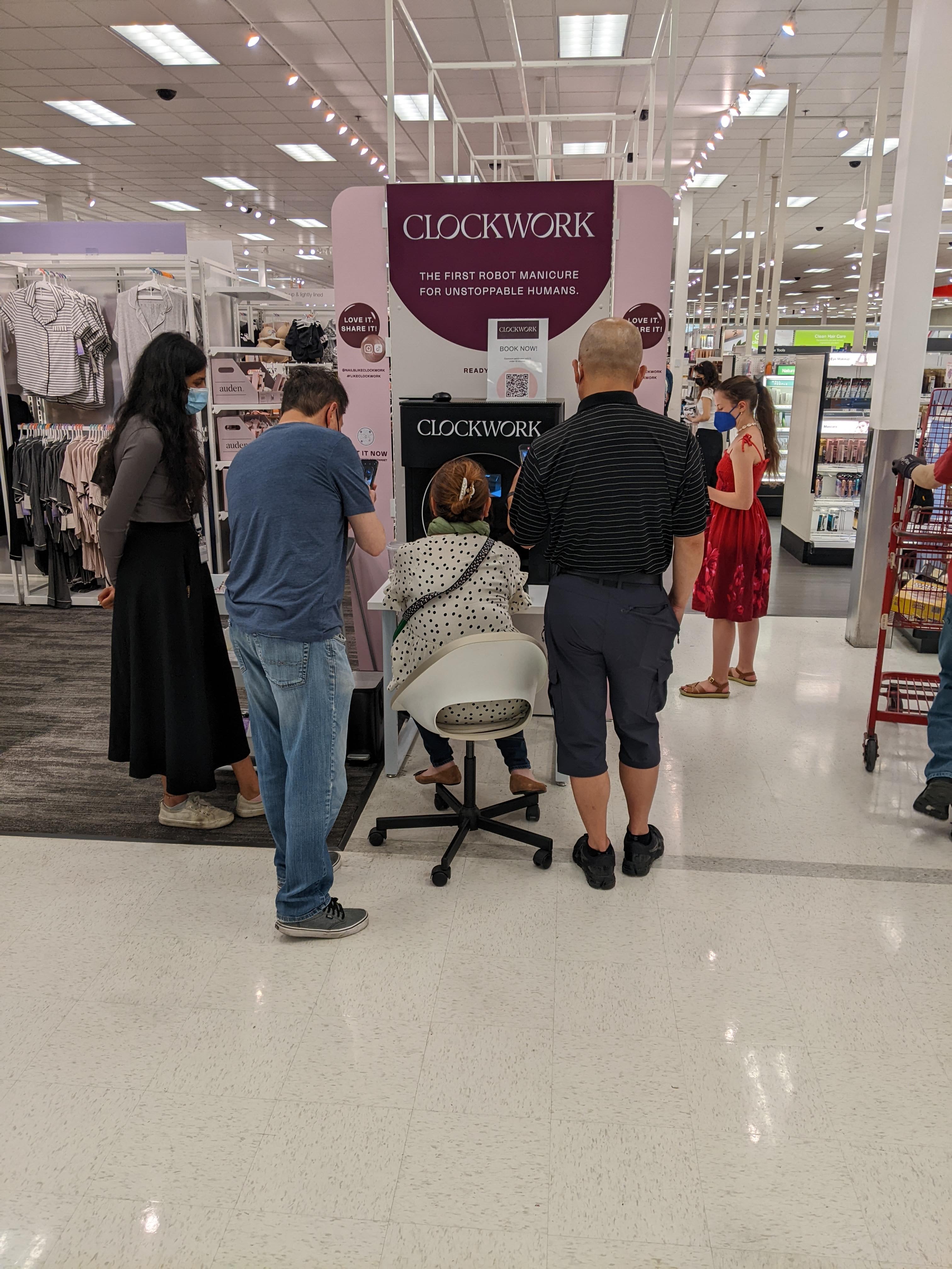
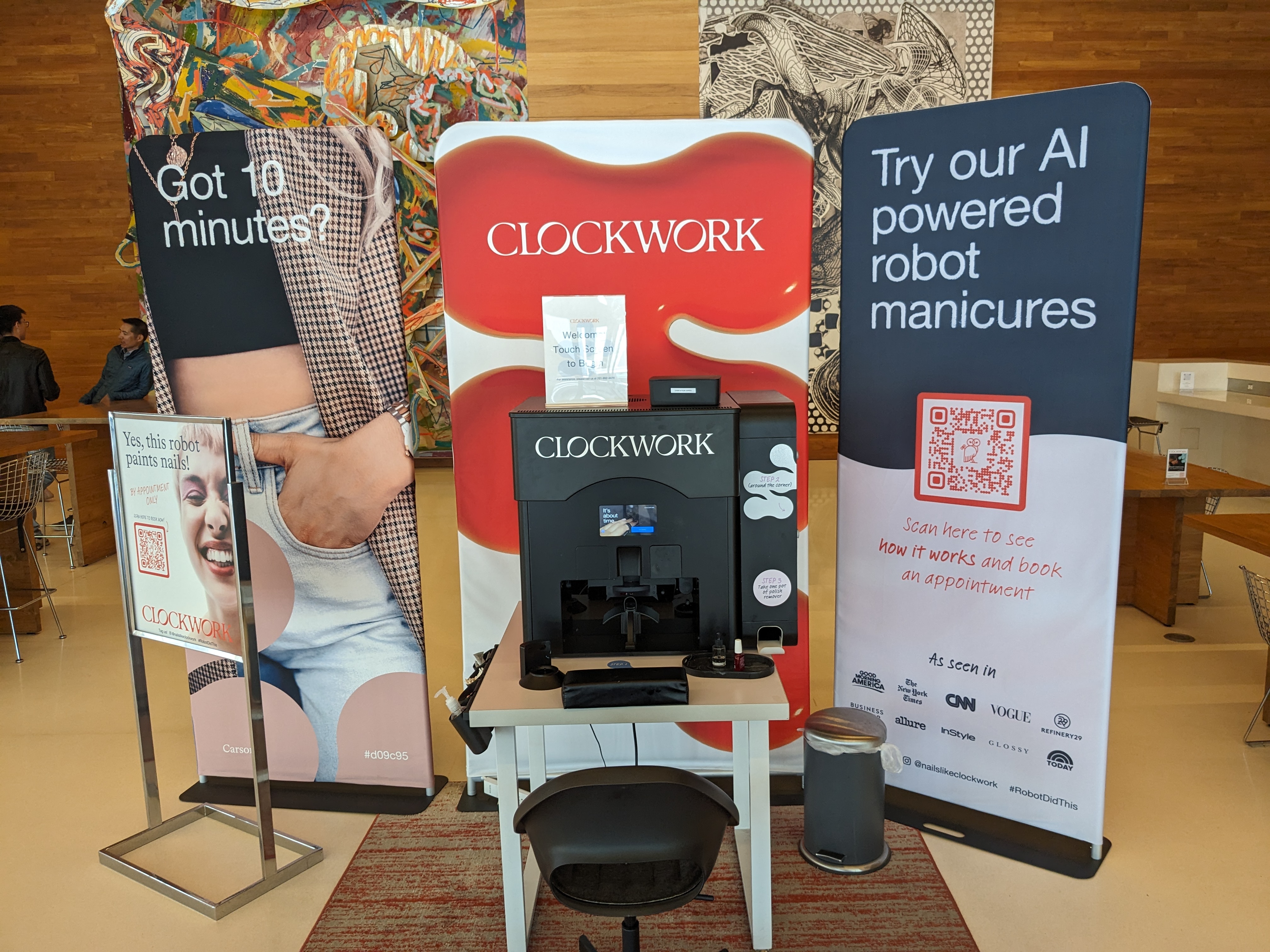
I built the world's first autonomous nail-painting robot, taking it from an early concept to a product deployed nationwide — the first working prototype came together in my home garage during the COVID-19 lockdown. As founding mechanical engineer I led the hardware design, prototyping, and production scaling: choosing and integrating the motion systems, fluid dispensing, material handling, and actuators that make the machine work, then setting up contract manufacturing, testing, and third-party servicing to keep it running in the field.

That work is behind the patent on the core application system (US10939738B2).

Arevo

Mechanical Engineer · 2014–2018 · Santa Clara, CA
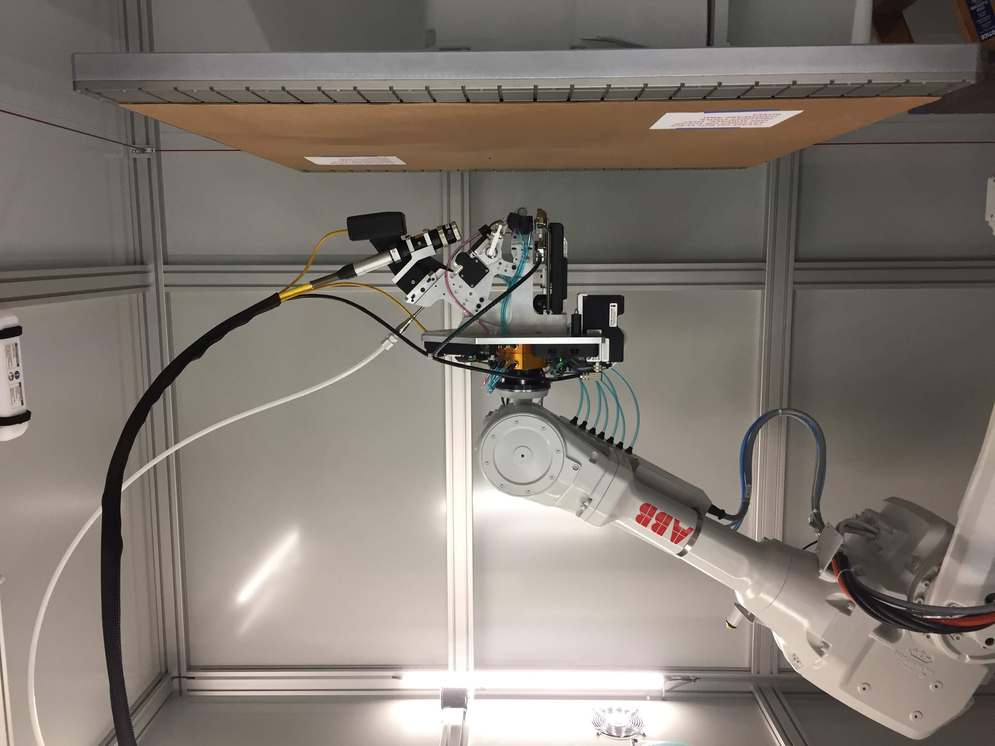
ABB robot arm fitted with a custom continuous carbon-fiber print head end effector
ABB ARM WITH CUSTOM PRINT HEAD END EFFECTOR

I worked on a 3D-printing system for large-scale continuous carbon-fiber parts, designing the print head end effector shown above — the mechanism that feeds, cuts, and handles the fiber material — around a mix of pneumatic and electric actuators. I fabricated and tested design iterations by hand to move fast, set up the company's PDM system for design documentation, and mentored engineers as the team grew from 6 to 40.

The filament guide and nozzle systems from that work became three patents (US10076870B1, US10926463B2, US10415898B2).

Nanosys

Mechanical Engineer · 2011–2014 · Palo Alto, CA

I built the precision deposition systems used to manufacture quantum-dot-enhanced optical films — the kind that ended up in Samsung displays and the Amazon Kindle Fire. That meant engineering equipment that could apply nanomaterials across large substrates at micron-level accuracy, prototyping components in an in-house machine shop, and working with contract manufacturers to scale the process.

Solyndra

Process Engineer · 2008–2009 · Fremont, CA

I worked the manufacturing line for Solyndra's novel cylindrical solar panels, improving yield and throughput while cutting costs. Most of that came down to better tooling for the automated systems, plus clearer process recipes and operator instructions for the floor.

Kiewit Pacific Co.

Engineering Estimator · 2006–2008 · San Francisco, CA

Before mechanical engineering, I estimated materials, labor, and equipment for large-scale bridge construction projects — early exposure to how big, physical things actually get built and budgeted.

SHEET 03 / 06

Patents

US10939738B2
Automatic Nail Polish Application System and Method
2021
US10926463B2
Grooved Guide for Providing Filament
2021
US10415898B2
Liquid-Cooled Fused Filament Fabrication Nozzle
2019
US10076870B1
Filament Guide
2018
SHEET 04 / 06

Skills & Education

CAD
SolidWorks, Autodesk Inventor
MFG & PROTO
CNC machining, mill, lathe, rapid prototyping, finishing tools
AUTOMATION
Motion systems, fluid dispensing, material handling, process automation, robotics
M.S. Mechanical Engineering
Georgia Institute of Technology
JULY 2006
Thesis: Nanomaterial Synthesis for Microsystem Integration
B.S. Mechanical Engineering
Georgia Institute of Technology
AUGUST 2004
Masters swimming / Tennis / Skiing / Inline skating / Paddling / Bike touring